Products Semiconductor / Diamond Substrates
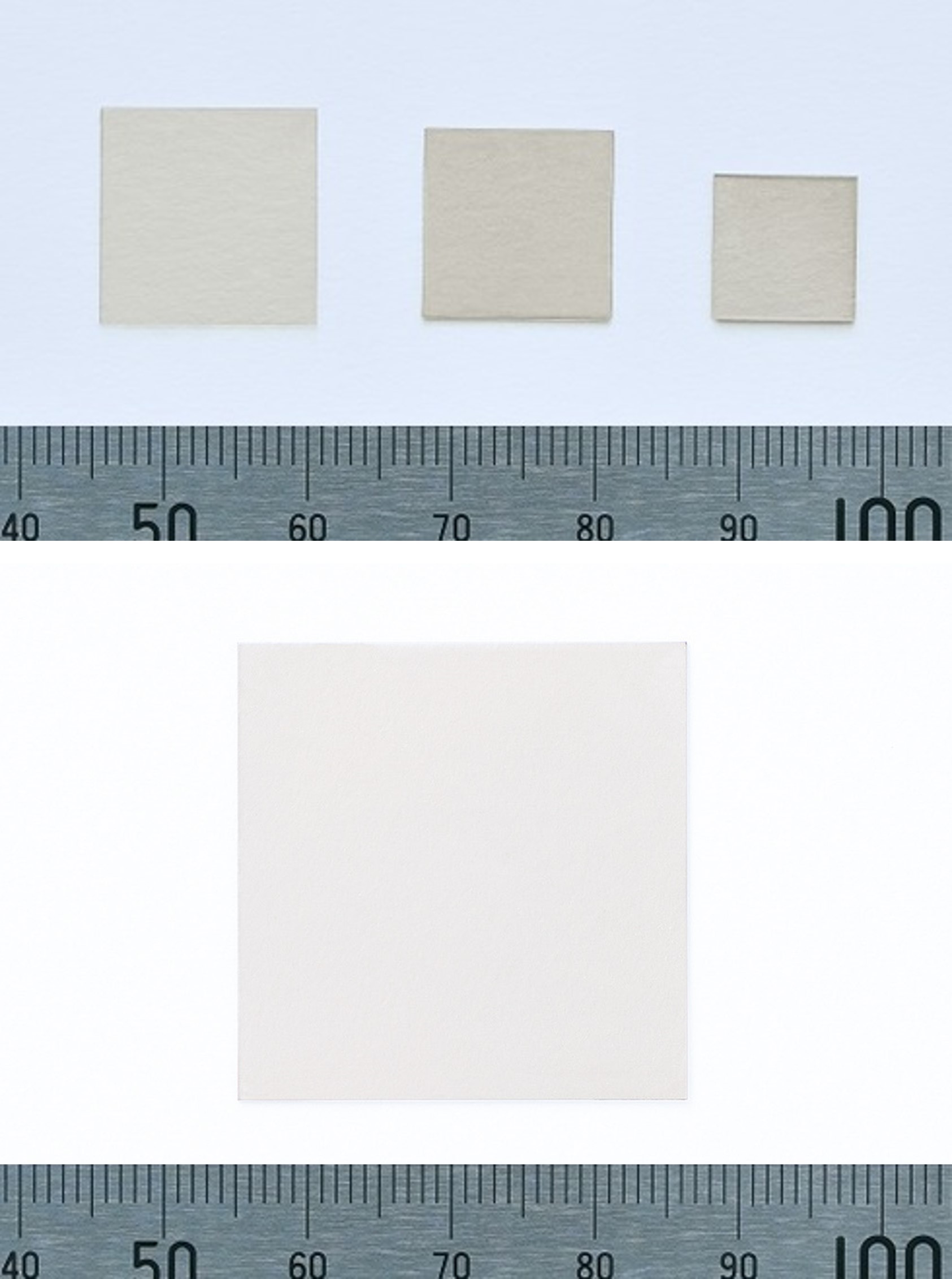
Single Crystal Substrates
| Standard Specifications |
|
|---|---|
| Special Specifications |
|
| High quality Substrate |
FWHM of X-ray locking curve can be selected. (ex. FWHM<50arcsec, FWHM<30arcsec) |
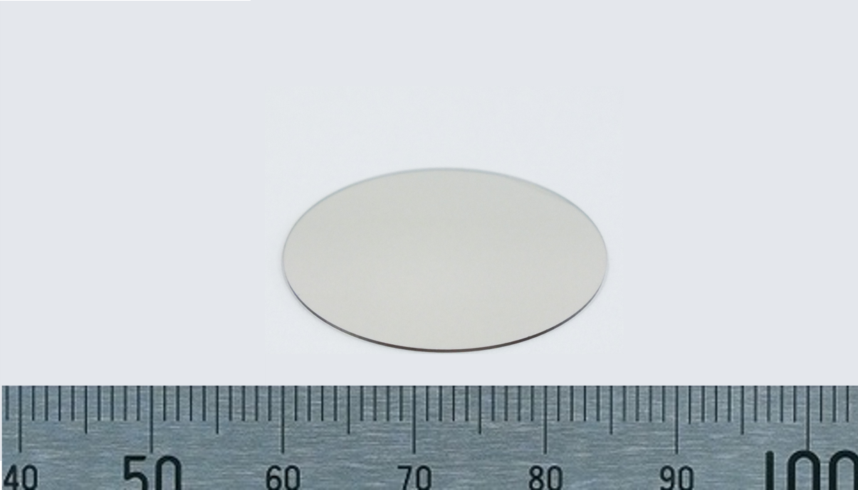
Mosaic Substrates
- *Joint from 2 to 9 single-crystal substrates that each size is 10 x 10mm.
- *Orientation is (100).
- * Size: <30x30mm, Thickness 0.03~3mm
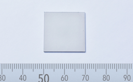
(111) Single Crisytal Substrate
| Standard Specifications |
|
|---|
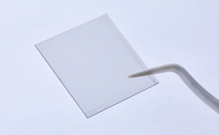
Heavy Bron-Doped Diamond Substrates
Free Standing Substrate
| B Concentration |
2×10²⁰ – 4×10²⁰/cm3 |
|---|---|
| Resistivity |
Less than 20mΩcm |
| Thickness |
0.2mm |
| Size |
Less than 13x13mm |
| Surface |
Both face polished (Ra<5nm or Ra<2nm) |
Heavy Bron Doped Epitaxial Substrate
| B Concentration |
2×10²⁰ – 4×10²⁰/cm3 |
|---|---|
| Thickness of boron doped layer |
0.03 – 0.2 mm (Polishing one face needs minimum 0.5mm thickness) |
| Largest size |
Single crystal less than 8x8mm, Mosaic crystal less than 18x18mm |
| Substrate |
Standard EDP substrate with thickness 0.3-0.5mm |
Epi-layer on Substrates
1. B-doped epitaxial layer
- B concentration:
- 2~10×1016/cm3
- Thickness:
- 0.5~10µm
- Mobility:
- 1500cm2/Vs or more
2. High purity epitaxial layer
- N concentration:
- <1ppm
- Thickness:
- 10~100µm
- Remarks:
- Can be done for Mosaic substrates Can be polished when thickness is more than 30 µm
We will offer various substrates for each customer inquiry.
Details of necessary specification will be required for your inquiries.
| Model Number | Size (mm) | Remarks |
|---|---|---|
| RH30303PP | 30×30×0.3 | Large Single-Crystal Substrate, both faces regular polishing |
| RH333Pf2 | 3×3×0.3 | Substrate with the off angle of 2° |
| RH555PP | 5×5×0.5 | Both faces regular polishing |
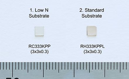
| RH333KPP | 3×3×0.3 | Standard Substrate, (111)Orientation, both faces regular polishing |
| RC333KPP | 3×3×0.3 | Low N Substrate, (111)Orientation, both faces regular polishing |
| RB552PP | 5×5×0.2 | Heavy bron doped substrate |
| RB443PPE20 | 4×4×0.3 | Heavy boron doped epitaxial layer 0.2mm on substrate |
| RH553PPN50PF | 5×5×0.3 | High purity epitaxial layer 0.05mm on substrate |
| RH20205PV | 20×20×0.5 | Mosaic substrate, one face regular polishing |
Contact Us
Please feel free to contact us about EDP
technology and products.
+81-661703871
Business Hours: Weekdays, 8:30am to 5:30pm (JST)